
Mapping stress in polycrystals with sub-10 nm spatial resolution.
- 5 September, 2017
- Publications
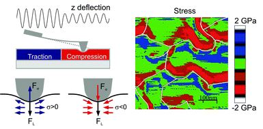 Mapping stress in polycrystals with sub-10 nm spatial resolution.
C. Polop, E. Vasco, A P. Perrino, et al.
Nanoscale, (2017).
Please Share This
Related Posts
Electron-phonon coupling in superconducting 1T-PdTe2
Electron-phonon coupling in superconducting 1T-PdTe2 Anemone, Gloria; Casado Aguilar, Pablo; Garnica, Manuela; et ál..…
Human-iPSC-Derived Cardiac Stromal Cells Enhance Maturation in 3D Cardiac Microtissues and Reveal Non-cardiomyocyte Contributions to Heart Disease
Human-iPSC-Derived Cardiac Stromal Cells Enhance Maturation in 3D Cardiac Microtissues and Reveal Non-cardiomyocyte Contributions to…
Extrinsic thermoelectric response of coherent conductors
Extrinsic thermoelectric response of coherent conductors Rafael Sánchez, Cosimo Gorini, and Geneviève Fleury Physical Review…
Photocatalytic Degradation of Fluoroquinolone Antibiotics in Solution by Au@ZnO-rGO-gC3N4 Composites
Photocatalytic Degradation of Fluoroquinolone Antibiotics in Solution by Au@ZnO-rGO-gC3N4 Composites Machin, A.; Fontanez, K.; Duconge,…
Bending Modulus of Lipid Membranes from Density Correlation Functions
Bending Modulus of Lipid Membranes from Density Correlation Functions Hernández-Muñoz,J.; Bresme,F.; Tarazona,P. and Chacón, E.…